SPI
The most reliable quality assurance solution
SPI is a advance guard to the quality management: the most effective means of improving production efficiency in the early stages of production
Mirtec's SPI has secured high precision and repeatability by adopting a leading optical technology, superior than other competitors. Based on this advantage,
the SPI can be used for general SMT as well as semiconductor productions as the SPI can detect the very minimal amount of solder paste
for defectives. In addition, Mirtec's diverse process management sofrware is a very effective way to optimize the process and improve production
efficiency by realizing problem on production and statistically analyzing the problem based on M2M communication with SPI.
 |
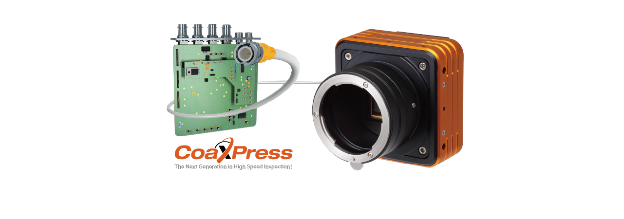
01. High-speed, High-precision inspection utilizing
|
|---|
 |
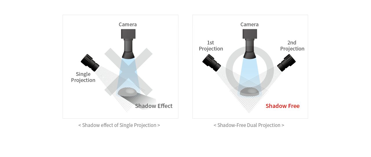
02. 3D measurement free from shadows and reflections测The Shadow-Free Dual Projection Moire Probe eliminates the possibility of distortion due to shadows when 3D measuring a high solder. By combining the pattern images of opposite direction, a perfect 3D measurements is possible and thus is free from reflective shadows. |
|---|
 |
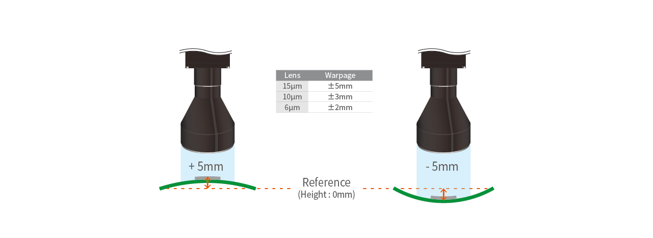
03. Bending and Warping Correction FunctionThe precise height measurement capability of the machine allows to automatically detect and correct bending states of PCB board. Normal inspections can be conducted on even bent or warped PCBs. |
|---|
 |
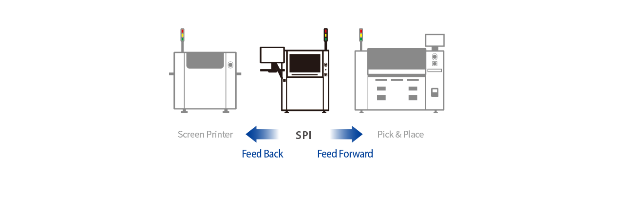
04. Closed-Loop SystemUsing real-time data communication from screen printers and mounter, the machine exchanges information like the pad and solder paste location to solve the source of defect and optimizes the process. |
|---|
Tel. +82-31-202-5999 Fax. +82-31-202-5990 E-mail. marketing@mirtec.com
Copyright(c)2017 MIRTEC CO., LTD. All rights reserved.